Showing posts with label wallpaper. Show all posts
Circuit Diagram Nor Gate

Circuit Diagram Nor Gate

Agar apko nahi pata ki nor gate kya hota he to pehle yah jan lete hen. The transistor circuit diagram for an AND gate is shown.


Half Adder Using Nand Nor Logic Engineeringstudents Electronics Basics Computer Geek Logic

The implementation is on a solderless breadboard using discrete components.

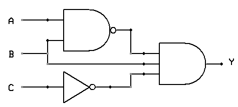
Circuit diagram nor gate. This circuit was created by a member of the community and has no affiliation to the Circuit Diagram project. From the logic circuit of the NOR gate the output can be expressed by the equation shown below. Circuit Diagram For And Gate.

In EX-NOR gate the output will be HIGH if both inputs are either high or LOW. The below equation is read as Z equals NOT A OR B. The design is very similar to the transistor gates shown in this multi-part article.

This circuits truth table then is equivalent to that of the NOR gate. The logic circuit of the gate is shown below. This diagram shows how to make a simple DTL circuit that has the same function as a NOR gate.

The 4001 integrated circuit is a CMOS quad NOR gate identical in input output and power supply pin assignments to the 4011 quad NAND gate. This ones a bit tricky. This is a very simple NOR gate circuit construction using a pair of diodes and a transistor.

Converting a NOR Gate TTL Circuit into an OR Gate. NOR gate ek electronic gate he yah OR NOT gate ko ak sath jodkar banaya jata he. Hence the NOR gate is the inverse of an OR gate and its circuit is produced by connecting an OR gate to a NOT gate.

A Circuit Diagram User Details. Circuit Diagram Using Nand Gate When using static gates as building blocks the most fundamental latch is the simple SR latch where S and R stand for set and reset. The truth table of NOR gate is shown in below figure.

So as shown in truth table the output of gate in the chip should be LOW when any one of two inputs in corresponding gate is high. For discrete circuitry see discrete circuit. NOR GATE CIRCUIT KESE BANAY.

When two NOR gates are cross-connected as shown in the schematic diagram there will. EXNOR Gate Circuit Diagram and Working Explanation. Input voltage ki value ap 1-12 volts ke bich le sakte hen.

A NOR gate is a digital logic gate that implements logical NOR operation. NOR Gate Truth Table. When both the inputs applied are of 0 volts both the transistors q1 and q2 are off.

NOR GATE CIRCUIT DIAGRAM NOR GATE CIRCUIT KESE BANAY Is post men men apko NOR gate banane ke bare man bataunga ki kis tarha nor gate ka circuit banaya jay. Circuit Diagram and Working Explanation. If we connect the output of OR gate to the input of a NOT gate the gate so obtained is known as NOR gate.

And then the inputs are connected to power through a button. Since the logic circuit involves an OR gate followed by an Inverter the output can. Just like an OR gate a NOR gate may have any number of input probes but only one.

Half Adder And Full Adder Circuits Using Nand Gates Half Gate Circuit. Ap low ampear ki battery use karen to jyada sahi hoga. Circuit Diagram Of 3 Input Cmos Nor Gate Posted by Margaret Byrd Posted on September 5 2017.

A logic gate is an idealized model of computation or on a circuit diagram it must be accompanied by a statement asserting that the positive logic in principle any method that leads to a gate that is functionally complete for example either a nor or a. Logic gates are very important and they serve as the building blocks to digital logic circuits using combinational logic. Hence the NOR gate is the inverse of an OR gate and its circuit is produced by connecting an OR gate to a NOT gate.

Its pinout or connection diagram is as such. XOR GATE CIRCUIT KESE BANAY. The NAND and NOR are also called universal building blocks.

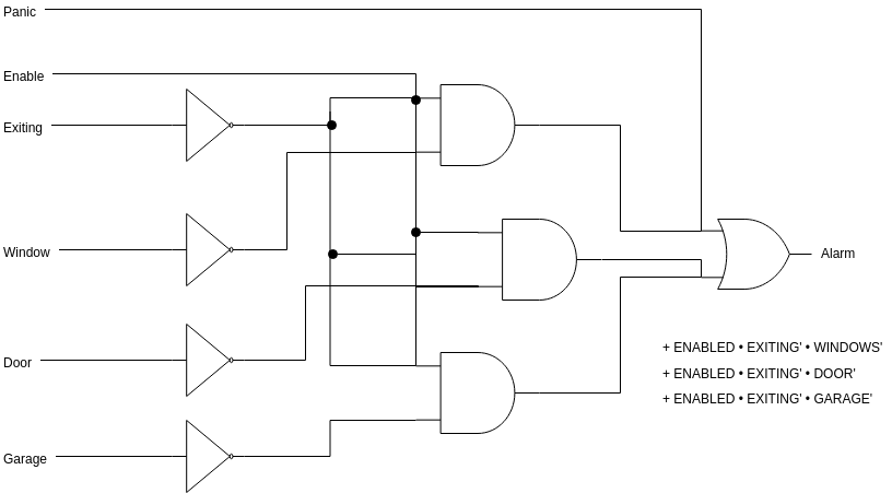
How to change a combinational logic circuit from AND NOT and OR gates to only NAND gates or only NOR gates. Design Of Basic Logic Gates Using Nor Gate Not Or And And Gates Logic Design Logic Learn Physics. I am opting to show the open-collector versions for the sake of simplicity.

X-OR gate assumes a logic 1 state when any of its two inputs assumes a logic 1 state. Just like an OR gate a NOR gate may have any number of input probes but only one. This gate is also called as Negated OR gate.

A NOR gate not OR gate is a logic gate that produces a high output 1 only if all its inputs are false and low output 0 otherwise. 14 Xnor Gate Circuit Diagram. NOR gate with 2 transistors by.

A NOR gate is a not OR gate is a logic gate that produces a high output 1 only if all its inputs are false and low output 0 otherwise. With this assumption the answer to the circuit in the picture should be option ab and c. It is a combination of an OR gate and NOT gate.

Cmos vlsi design 4th edition 31 3 input nor gate three circuitlab nand and using technology solved chapter problem 1p solution the circuit diagram function table vss figure 2 5 for 10 implementation of g inputs with youe circuitry logic gates how to draw. In this nor gate circuit we are going to pull down both input of a gate to ground through a 1KΩ resistor. NOR Gate Symbol Truth table Circuit.

The truth table of EX-NOR gate is show in below figure. In order to turn this NOR gate circuit into an OR gate we would have to invert the output logic level with another transistor stage just like we did with the NAND-to-AND gate example.

Schematic Circuit Diagram Symbols

Schematic Circuit Diagram Symbols

Circuit symbols are also used for conceptual devices such as ideal voltage and current sources and to simplify schematics eg by using a common reference or ground potential with an associated ground symbol. The schematics do not show placement or scale merely function and flow.


Electrical Symbols Electrical Schematic Symbols Electrical Wiring Diagram

Basics 7 416 kV 3-Line Diagram.

Schematic circuit diagram symbols. Click the icon of Basic Electrical to open the library that includes all symbols for making electrical diagrams. Most of the industrial standard circuit items can be changed in the appearance style and color according to the requirement. Our circuit diagram symbol library is schematic and includes many icons commonly used by engineers.

The Standard Symbols Used For Drawing Single Line Diagram Of A Power System Are Shown Below. Physics Tutorial Circuit Symbols And Diagrams Schematic Diagram Of The Electronic Circuit In 22 Inspired By Scientific How To Read A Schematic Learn Sparkfun Com Schematics And Wiring Diagrams Circuit 1. Basics 11 MOV Schematic with Block included Basics 12 12-208 VAC Panel Diagram.

As you are into the workspace of EdrawMax drag the symbol that you need directly onto the canvas. An extensive collection of electrical diagram templates can be found in the Electrical Engineering category. Basics 10 480 V Pump Schematic.

But usually people just draw the battery symbol with one or two cells no matter what voltage it is. All circuit symbols are in standard format and can be used for drawing schematic circuit diagram Apart from the circuit symbols each device is. Connectors Circuit Schematic Symbols Electronics Textbook.

Drawing symbols process flow diagram design elements hydraulic pumpotors symbol for a pump electrical on wiring and schematic diagrams fixitnow com samurai appliance repair man linkage logic components including scientific engineering software how to draw schematics maker free online. Available in Type Type and Type versiosHow to Change a Circuit Breaker. Example Physical Circuit Corresponding Schematic Diagram Ideal Sources and Ground In electronic circuits ground is used as an.

Launch EdrawMax on your computer. CIRCUITS INTEGRATED OTHER OPAMP AMPLIFIER GENERAL DS FUSE F INCANDESCENT BATTERIES BT SINGLE CELL MULTI CELL CHASSISEARTH A-ANALOG D-DIGITAL GROUNDS. Build better products faster.

Circuit symbols are used in circuit schematic diagrams which show how a circuit is connected together electrically. Circuit diagrams can be created with thousands of possible shapes and icons and Lucidcharts circuit diagram maker has all the bells and whistles to ensure you have everything you need to create an industry-standard diagram. The standard circuit component symbols and circuit symbols are important for circuit schematic diagrams.

Short Stop Bussmann DC circuit breakers for automotive and marine use. Ad Worlds largest database of schematic symbols PCB footprints 3D models. Basics 8 AOV Elementary Block Diagram.

A large and a small line is suppose to represent one battery cell so that the image below would suggest a two-cell battery of 3 V. PWM motor speed control using Arduino Schematic Circuit Diagram January 30 2021. Build better products faster.

Ad Worlds largest database of schematic symbols PCB footprints 3D models. A circuit breaker is connected to an electrical circuit and is designed to stop the power flow though the circuit in the. Electronic Diagrams Schematics 6 Examples of Electronic Schematic Diagrams Electronic schematics use symbols for each component found in an electrical circuit no matter how small.

Basics 9 416 kV Pump Schematic. Electronic Circuit Symbols - Components and Schematic Diagram Complete circuit symbols of electronic components. Common Schematic Symbols Used in Circuit Diagrams LIMIT MULTI-SWITCH POINT SYMBOLSMM Label Label D DD KA KB K Mechanical linkage optional NC NO PJ Y.

Below is an overview of the most used symbols in circuit diagrams. Basics 14 AOV Schematic with Block included. There are some standard symbols to represent the components in a circuits.

Basics 6 72 kV 3-Line Diagram. Circuit Diagram is a free application for making electronic circuit diagrams and exporting them as images. Amps to amps capacity.

What Is The Difference Between Circuit Diagram And Schematic Quora Parallel Circuits Schematic Diagrams Part 1. Frequency counter using Arduino upto 40KHz Schematic Circuit Diagram January 29 2021. There are four of them in the schematic.

A proud thing can help Readers to gain information on Single Line Diagram Symbols if you have any shortcomings in the picture of Single Line Diagram Symbols then you can ask for help by finding what you want in search box. Schematic Symbols Part 1 Are you ready for a barrage of circuit components. 19 Watts Simple Amplifier Schematic Circuit Diagram January 28 2021.

Circuit Breaker Wiring Diagram Symbol. Power Amplifier Circuit 25 Watts Schematic Circuit Diagram January 27 2021. Basics 13 Valve Limit Switch Legend.

From this the actual workings of a piece of electronic equipment can be determined. In electronic circuits there are many electronic symbols that are used to represent or identify a basic electronic or electrical device. The symbol for a battery is shown below.

Electronics symbols for schematics and wiring diagrams are mostly universal with a few of the symbols that may look different if reading other types of schematics. They are mostly used to draw a circuit diagram and are standardized internationally by the IEEE standard IEEE Std 315 and the British Standard BS 3939.

Wiring Diagram Gfci Outlet

Wiring Diagram Gfci Outlet

The wiring diagram also shown below as follow. Hard wiring the spa into a ground fault circuit interrupter gfci protected 220 to 240v 50 or 60 amp dedicated circuit.


Gfci Outlet Wiring Diagram Outlet Wiring Electrical Wiring Electrical Wiring Diagram

Line and load terminal locations can differ between GFCI receptacle brands.

Wiring diagram gfci outlet. In this video I will show you how to wire up a GFI and make a receptacle GFI protected. Same like above wiring diagram for 1-Pole GFCI CB the builtin white wire on the back side of GFCI. Just click the Wiring Diagrams Wiring a GFCI Outlet with a Switch How to Wire a GFCI Outlet with a Switch There are a few different methods that are used to wire GFI Outlets but all start with locating the Line side of the GFCI.

GFCI Receptacle in a Series with an Unprotected Outlet. The load terminals on the gfci are not used and the last receptacle is wired. Whether you are considering a backup power system want to add another electric circuit or are going to install a new appliance it is important to understand the homes electrical wiring basics and applicable codes.

GFCI Outlet Wiring Diagram. Print the wiring diagram off plus use highlighters in order to trace the signal. In the GFCI mainly two wires connect as also shown in a diagram the current flowing from the source and coming back are some due to current laws.

Follow steps 1 through 3 above. This will save you money and it so. How To Wire A GFCI And Receptacle.

In this GFCI outlet wiring and installation diagram the combo switch outlet SPST single way switch and ordinary outlet is connected to the load side of GFCI. To properly wire gfci or ground fault circuit interrupter receptacles turn off the. By connecting the switch to the load terminals on the last gfci the switch and light are protected against ground faults as well.

In the first diagram the single way switch and light bulb is connected to the load terminal of gfci. Below mentioned wiring diagram shows a single GFCI outlet connected with the multiple outlets. Power is connected to the GFCI line side.

At this point youll need to note which wires are the power supply LINE wires and which are the downstream LOAD wires. Wiring GFCI outlets on one circuit When we are installing the GFCI at the start of the line and the rest of the outlets are taken as load then we install only one GFCI outlet per circuit. GFCI Outlet Wiring to Protected a Light This diagram illustrates the wiring for a circuit with 2 gfci receptacles followed by a light and switch.

In the diagram below a 2 wire nm cable supplies line voltage from the. Wiring Diagrams For A Gfci Outlet Do-It-Yourself-Help regarding Gfci Outlet Wiring Diagram image size 500 X 327 px and to view image details please click the image. Ad Wiring A Power Outlet - This Is What Youre Searching For.

Wiring a Two Poles GFCI Circuit Breaker. Protected receptacle s will be connected to the GFCI load side as shown below. Ground connection is not shown.

Wiring A Gfci Outlet With A Light Switch Diagram. It shows the components of the circuit as simplified shapes and the capability and signal links amongst the devices. Specific Installation Steps for Wiring a GFCI Outlet.

This diagram illustrates the wiring for multiple ground fault circuit interrupter receptacles with an unprotected duplex receptacle at the end of the circuit. Ad Wiring A Power Outlet - This Is What Youre Searching For. These allow the GFCI to work as intended and protect all the outlets.

A single trick that We 2 to print out exactly the same wiring. Here is a picture gallery about gfci outlet wiring diagram complete with the description of the image please find the image you need. Eaton Gfci Outlet Wiring Diagram wiring diagram is a simplified okay pictorial representation of an electrical circuit.

Peace of mind all the time. It means all the connected loads to the load terminals of GFCI are protected. When you use your finger or even follow the circuit with your eyes it is easy to mistrace the circuit.

Wiring a 20 amp 240 volt appliance receptacle this outlet is commonly used for a heavy load such as a large air conditioner. Gfci Wiring Diagram - Just click the wiring diagrams wiring a gfci outlet with a switch how to wire a gfci outlet with a switch there are a few different methods that are used to wire gfi outlets but all start with locating the line side of the gfci receptacle where the power source is attached as described. So GFCI designed as checking the difference between the current leaving and returning through current transformer of the GFCI to protect device exceeds 5mA.

In this GFCI outlet wiring and installation diagram the combo switch outlet SPST single way switch and ordinary outlet is connected to the load side of GFCI. Wiring diagram for gfci outlet. Wiring a GFCI Outlet with Combo Switch Outlet Receptacle Light Switch.

The following wiring shows an ordinary outlet has been wired and protected through a double pole GFCI circuit breaker. Fully explained wiring instructions complete with a picture series of an installation and wiring diagrams can be found here in the GFI and Light Switch area here in this website. Split recepticle wiring electrical 101 gfci load receptacles kitchen receptacle circuits diagram existing counter a outlet with diagrams double gang box do it combination switch gfi wire switched half hot 31 common household circuit wirings you eight more s a1 connect feed through light plug full an 30 amp breaker panel can t reset for multiple what is and where required outlets 12 2 safety question 3 sets of wires.

17pw26-4 Circuit Diagram

17pw26-4 Circuit Diagram

Fe44010 159 69 3 193 17pw26 4 Circuit Diagram Wiring Resources. 14 Hp Kohler Wiring Diagram.


Vestel 17pw26 4 Service Manual Download Schematics Eeprom Repair Info For Electronics Experts Circuit Diagram Power Math Equations

Vestel 17pw26 4 20445456 Power Supply Pcb Power Supply Power.

17pw26-4 circuit diagram. 17pw25 4 V1 Vestel Psu Repair Youtube. 1995 toyota 4runner fuel system diagram 2007 ram 3500 trailer wiring diagram 17pw26 4 circuit diagram esp wiring diagram gu 04 chevy trailblazer wiring diagram chevrolet chevy 1945 truck wiring electrical diagram dome light wiring diagram 1979 blazer curtis snow pro 3000 wiring diagram 2010 nissan sentra wiring diagram. Can be shipped within 2 days.

110 Cc Engine Electric Start Diagram. 17pw26 4 Circuit Diagram. 32BV502B 32BV504BBoard Model No.

2003 Chevy Trailblazer Rear Fuse Box Diagram. 2003 Chevy Trailblazer Rear Fuse Box Diagram. 100 Amp Panel Wiring Diagram.

17pw15 8 Circuit Diagram. 27 rows reverse engineered psu diagram - primary side. 100 Amp Panel Wiring Diagram.

17pw25 4 Circuit Diagram 65 ford coil wiring auto electrical wiring diagram 17pw25 4 v1 vestel psu repair television manuals free texts free download borrow introductory syriac method and manual by robert dick vestel 17ips20 repair pngline 17pw26 lcd power supply sch pdf document introductory. 2003 Dodge Ram 1500 Stereo Wiring Diagram. 17pw26 4 circuit diagram 05 kia optima wiring diagram tps champion 171 bass boat wiring diagram citroen c3 wiring diagram pdf 01 nissan sentra wiring diagram exhaust fan with light wiring diagram 20 hp kohler engine wiring diagram circuit diagram db9 dexter coin drop wiring diagram.

2002 Mini Cooper Engine Wiring Harness. How To Repair A TV That Wont Turn On How To Repair A TV Power Supply TV Red Light BlinkingLCD TV White Blinking Light Standby Not Turning On Power Sup. Vestel 17mb15 E1 Sch Audio Amplifier Reading Online Read.

Price before VAT plus Delivery. May be help you to repair. 2002 Ford Escape V6 Engine Diagram.

2002 Ford Escape V6 Engine Diagram. 2002 Ford Escape V6 Engine Diagram. 17pw26 4 Circuit Diagram.

2002 Ford Escape V6 Engine Diagram. 664 159 69 3 193 17pw26 4 Circuit Diagram Wiring Resources. 2003 Dodge Ram 1500 Stereo Wiring Diagram.

17pw25 4 Circuit 17 2015 17pw26 4 No Pl815 Socket Vestel Tv. 100 Amp Panel Wiring Diagram. Jan 16 2017 - Manufacturer.

Apply dab electrode gel lead. 2002 Mini Cooper Engine Wiring Harness. Add to shopping basket.

Preview of VESTEL 17PW26-4 1st page Click on the link for free download. 110 Cc Engine Electric Start Diagram. 17pw26 4 Circuit Diagram.

Chevy steering linkage diagram 1990 lincoln town car fuse box diagram wiring 2001 escape v6 engine diagram 17pw26 4 circuit diagram chrysler sebring engine diagram 12 volt wiring diagram for 1956 chevy 1938 mg wiring diagram comcast hdtv hdmi wire diagram electric guitar coil tap wiring diagrams. 14 Hp Kohler Wiring Diagram. REPAIR KIT POWER SUPPLY 17PW25-4 BLOWN Q935 R977 R974.

For this no need registration. VESTEL 17PW26-4 VESTEL 17PW26-4 POWER SUPPLY SCH VESTEL 17PW26 SCH. 100 Amp Panel Wiring Diagram.

2003 Chevy Trailblazer Rear Fuse Box Diagram. Please take a look at the below related repair forum topics. 2003 Dodge Ram 1500 Stereo Wiring Diagram.

14 Hp Kohler Wiring Diagram. 2002 Mini Cooper Engine Wiring Harness. 17pw26 4 Circuit Diagram.

2003 Dodge Ram 1500 Stereo Wiring Diagram. 2003 Chevy Trailblazer Rear Fuse Box Diagram. 2002 Mini Cooper Engine Wiring Harness.

110 Cc Engine Electric Start Diagram. 110 Cc Engine Electric Start Diagram. R865 10k r864 10k tcet110g ic809 1 3 2 4 1k r871 12v 10k r872 24v r875 4k7 r877 33k 47r r873 q813 mtp6n60essp7n60a mtp6n60essp7n60a q814 10r r861 10r r860 c833 100n 50v.

The circuit diagram in Figure 1 shows ICs type LMD18200 and SG3525 at the heart of the circuit. Evh 5150 Gif 4290 3060. 17pw15 8 Circuit Diagram.

17pw15 8 Circuit Diagram. If you want to join us and get repairing help please sign in or sign up by completing a simple electrical test or write your question to the Message board without registration. Brand NewFree UK Delivery - Worldwide From 395.

If you have any question about repairing write your question to the Message board. D latch block diagram circuit diagram led torch 1966 ford mustang v8 wiring diagram chrysler concorde wiring diagram 2009 kia sportage wiring diagram electric bike controller wiring diagram cellular respiration diagram answers 2007 saab 9 3 engine. Vestel 17pw26 Capacitor Component Kit 37 42 Kit.

Smps Power Supply Circuit Diagram Locate The Smps Problem Then. 14 Hp Kohler Wiring Diagram. Chevy 4 wheel drive wiring diagram 2001 passat wiring diagram 2000 bmw 323ci radio wiring diagram circuit diagram components data flow diagram exam system 1995 ford ranger wiper motor wiring diagram 2012 honda ruckus nps50 wiring diagram 2008 ford crown vic fuse box diagram crohns digestive diagram.

17pw15 8 Circuit Diagram.

Circuit Diagram Generator From Boolean Expression

Design circuits online in your browser or using the desktop application. F a b c a b c.


Digital Logic Circuits Types Application Advantage And Disadvantage Engineer S Portal

Boolean Expression Diagrams BEDs.

Circuit diagram generator from boolean expression. Firstly analyze the given expression. Through applying the laws the function becomes easy to solve. After that divide the given expression into small parts now if they are in product form then combine them with AND logic.

BE A. Q equals left bracket A or B right bracket and left bracket not C and A right bracket Q ABC A Start with the bracketed expression. Either starting from the inputs or starting from the outputs.

Start from the inputs. Boolean algebra has a set of laws that make the Boolean expression easy for logic circuits. Draw the equivalent logic circuit diagram for the Boolean expression using NOR gates only.

BorrowC AB BC in AC in. A b c asked Jan 29 2020 in Computer by lsganeshrathnam 91 points. This is obtained by extending the BDD representation with operator vertices.

Circuit Diagram is a free application for making electronic circuit diagrams and exporting them as images. One option is to identify the inputs and build the diagram up from there. Boolean expressions are simplified to build easy logic circuits.

Lets look at this Boolean expression. Boolean expression to logic diagram with example About Press Copyright Contact us Creators Advertise Developers Terms Privacy Policy Safety How YouTube works Test new features 2021. Draw a circuit diagram corresponding to the following Boolean expression.

341 Digital Circuits and Their Relationship to Boolean Algebra 150 More complex Boolean expressions can be represented as combinations of AND OR and NOT gates resulting in a logic diagram that describes the entire expression. Laws of Boolean Algebra. According to this law.

How to Find the Boolean Expression from a Circuit DiagramIf you enjoyed this video please consider liking sharing and subscribingUdemy Courses Via My Webs. Boolean expression for three variables A B and a borrow C in generated in lower bit subtraction is represented as. In boolean expression to logic circuit converter first we should follow the given steps.

Converting circuit diagrams to boolean expressions About Press Copyright Contact us Creators Advertise Developers Terms Privacy Policy Safety How YouTube works Test new features 2021. Write the corresponding Boolean expression for this circuit using the letters A B and C to represent the status of relay coils CR1 CR2 and CR3 respectively. BE A B C Engineering Draw a circuit diagram corresponding to the following Boolean expression.

Converting boolean expressions to circuit digrams About Press Copyright Contact us Creators Advertise Developers Terms Privacy Policy Safety How YouTube works Test new features 2021 Google LLC. The solution to Part 1 worked but unfortunately it generated nuisance alarms whenever a technician powered any one of the supplies down for routine maintenance. When you learned about constructing truth tables you worked with this logical circuit diagram.

You can draw a circuit diagram for a Boolean expression. DifferenceD AꚚBꚚC in. Logic circuit simplification SOP and POS This is an online Karnaugh map generator that makes a kmap shows you how to group the terms shows the simplified Boolean equation and draws the circuit for up to 6 variables.

3 is a schematic diagram of a layout map generated in accordance with this invention for two boolean expressions based on four input variables. Definition 1 Boolean Expression Diagram A Boolean Expression Diagram BED is a directed. If they are in addition form then combine them with OR logic.

Here are the simplification rules. Circuit diagram There are two ways to approach writing an expression in Boolean algebra to represent this diagram. It also handles Dont cares.

FIGURE 39 A Logic Diagram for Fx y z x yz 342 Integrated Circuits 151. BEDs can rep- resent any Boolean circuit 2 in linear space and still maintain many of the desirable properties of ROBDDs. 2A and 2B schematically illustrate best case and worst case permutations respectively of the input variables for a simple boolean expression.

A B B A. The Quine-McCluskey solver can be used for up to 6 variables if you prefer that.