Showing posts with label logic. Show all posts
+13 Logic Circuit Diagram References

+13 Logic Circuit Diagram References


+13 Logic Circuit Diagram References. In simple terms, logic gates are the electronic circuits in a digital. Truth tables circuit diagrams of logic gates.

Draw a Logic Circuit in CircuiTikZ TikZBlog
Draw a Logic Circuit in CircuiTikZ TikZBlog from latexdraw.com

Web what is a logic circuit diagram? When you hold ctrl key you can drag any empty space on the diagram to. Free circuit diagram maker edrawmax online.

Circuit Diagram Of Calculator Using Logic Gates

Circuit Diagram Of Calculator Using Logic Gates

If shift right by one position it is equivalent to multiplying by 2. Or gate diode circuit diagram.


Pin On Furniture

Frequency counter using Arduino upto 40KHz Schematic Circuit Diagram.

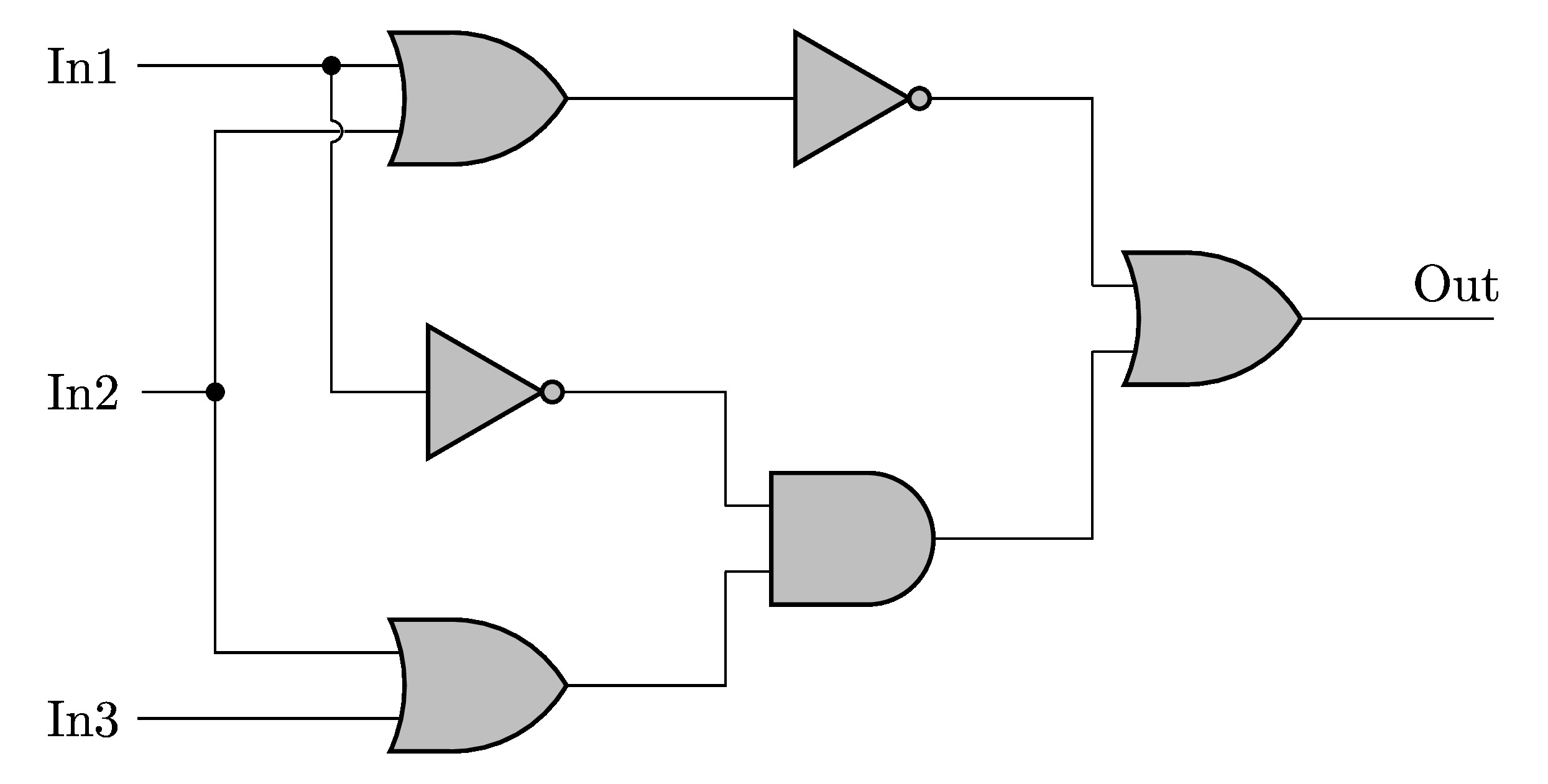
Circuit diagram of calculator using logic gates. No matter you want a logic diagram tool for teaching or a logic circuit software for engineering purposes our online logic diagram. A logic gate is really just a simple electrical circuit that compares two numbers inputs and produces a third number an output depending on the values of the original numbers. Page on 1at pre.

In order to make a full adder we have to use 2 XOR gates 2 AND gates and an OR gate. Mini Audio Amplifier Schematic Circuit Diagram. There are four very common types of logic gates.

Is it a binary calculator. Creation of a circuit from logical elements construction of a truth table by a Boolean function and Karnaugh map editor. This is then repeated for a couple more times for debouncing.

A keypad decoding logic circuit is also a pretty complicated combinational circuit and even more when you have to implement debouncing. Circuit Diagram Of Calculator Using Logic Gates. The logic gate software has all the logic symbols you need to design any kind of logic model.

The full adder works by putting inputs A and B through a XOR gate then taking the output from that and XORing it with the Carry-in. It uses logic gates to compare the pattern of switches that are active and come up with a new pattern of switches instead. Low Cost 150 Watt Amplifier Schematic Circuit Diagram.

Mini Audio Amplifier Schematic Circuit Diagram. Need to draw logic gate diagrams. Is it a decimal calculator.

How does the calculator do the actual sum. Logic gate circuits are most frequently symbolized with a schematic diagram through their own exclusive symbols. Hi Fi Amplifier Circuit 2X12 Watts Schematic Circuit Diagram.

Simple Circuit Diagram Of Digital Clock Using Logic Gates. Appendix A Logic Gates And Boolean Algebra In The Book Fsm Based Digital Design Using Verilog Hdl. Digital alarm clock using 4026 logic 24 hour and timer circuit 12h 24h online how to make a simple diagram of ic 555 based on sam gordon theory multisim an old school nuts simulation design.

I am going to show you how to make a 4 bit 0-15 adding calculator using 74xx series IC chips. THIS USES LOGIC DEVICES. 8 Best Free Truth Table Calculator Software For Windows.

A combination of gates make up a circuit and some digital circuits can be extremely complex. X-OR gate assumes a logic 1 state when any of its two inputs assumes a logic 1 state. We need a full adder.

Power Amplifier Circuit 25 Watts Schematic Circuit Diagram. The Exclusive Or Function Xor Gate Boolean Algebra Electronics Textbook. Thanks for quest The Calculator what your looking for is not clear Usage Logic gates it all depend on whats your requirement.

Visual Paradigms logic diagram tool features a handy diagram editor that allows you to draw logic diagrams swiftly. It is the combination of AND gate followed by an inverter. Basically logic gates are the elementary electronic logic circuit that can make a variety of different types of circuits by the interconnection of these three gates to perform complex logical operations of any computer.

Logic 0 Low 0V. An X-OR gate is a two-input one output logic circuit. Multiplication is done by shift registers.

PWM motor speed control using Arduino Schematic Circuit Diagram. Frequency counter using Arduino upto 40KHz Schematic Circuit Diagram. And again how much Digit of the inputs.

For addition you have adder circuit using logic gates. The circuit for the full adder is shown below. But if you are a human then this is only a fun project.

Digital Alarm Clock Using 4026 Logic Gates. PWM motor speed control using Arduino Schematic Circuit Diagram. The time of the pulse is set by 2 components.

This gives you the bit output. NOR or NAND gates. Logic 1 High V.

If you shift left a binary number one position it is equivalent to division by 2. The output of the X-OR gate will be the sum of the modulo sum of its inputs. If you want to quickly add numbers from 0 to 15 and you know how to rapidly convert into binary and back into decimal this is for you.

19 Watts Simple Amplifier Schematic Circuit Diagram. Logic circuit editor The service consists of three types of calculator. Power Amplifier Circuit 25 Watts Schematic Circuit Diagram.

When both the inputs assume the logic 0 state or when both the inputs assume the logic 1 state the output assumes a logic 0 state. Keypads columns are polled repeatedly and when a key is pressed the poll returns a positive result which would reflect the row. Subtraction is done by adding the complemented number.

Introduction To Digital Logic Book Chapter Iopscience. This monostable is built around 2 LOGIC gates. It produces an output pulse either high or low by using.

Schematics Com Boolean Algebra Calculator. Looking for a logic circuit tool. Posted by Margaret Byrd Posted on July 30 2021.

19 Watts Simple Amplifier Schematic Circuit Diagram. The first program allows to create an online circuit of logic elementsAccording to the constructed circuit diagram there are CNF DNF Zhegalkin normal form. Logic Circuit Diagram NAND Gate As per the above circuit connection between diodes and an NPN transistor the circuit for the NAND gate is designed.

Circuit Diagram Using Logic Gates

Circuit Diagram Using Logic Gates

The following table shows the truth table of 2-input AND gate. In this post you will practise drawing logic gates diagrams using the following logic gates.


Basic Logic Gates Using Nand Gate Not Or And Gates Nand Gate Logic Basic

Posted by Margaret Byrd Posted on July 30 2021.

Circuit diagram using logic gates. Back on the Ben Heck Show a viewer requested a real-life build of the game from Jumanji. In this post we will see how basic digital gates can be made with the help of diodes and transistor. Current does not flow to the output unless both switches are closed.

It is the combination of AND gate followed by an inverter. Most logic gates can be made quite easily with transistors. Traffic Lights Circuit Design Using Logic Gates Posted by Margaret Byrd Posted on July 31 2021 Traffic lights circuit implemented on joe s hobby electronics simple four way light using two 4 tutorial diagram 555 digital logic design educoder experiment.

A much better way is to use algebraic expression. By the use of two Half Subtractors called a cascading technique these Full subtractors can be constructed. Furhtermore a bar over a variable or a in front of the variable represents an.

This is a FM Transmitter circuit. The basic gates are AND OR NOT gates. Logic Gates Diagrams 101 Computing.

We can implement the above Boolean functions using logic gates. The output of the X-OR gate will be the sum of the modulo sum of its inputs. The transistor circuit diagram for an AND gate is shown below.

When both the inputs assume the logic 0 state or when both the inputs assume the logic 1 state the output assumes a logic 0 state. DTL NAND Circuit The DTL NAND gate combines the DTL inverter with a simple Diode-Resistor Logic DRL AND gate as shown in its circuit diagram. This oscillator uses 107Mhz ceramic filter and inverter N2 to drive the parallel combination of N4 to N6 through N3.

AND Gate Transistor Circuit Diagram. Here a dot represents the AND operation and a represents and OR operation. Logic Circuit Diagram NAND Gate As per the above circuit connection between diodes and an NPN transistor the circuit for the NAND gate is designed.

In the above circuit when A or B or both A and B are grounded or at 0V potential transistor T 1 or T 2 or both T 1 and T 2 are in OFF condition respectively. Circuit Diagram Using Nand Gate. An AND gate is a digital circuit that has two or more inputs and produces an output which is the logical AND of all those inputs.

This transmitter circuit has a RF oscillator. In the circuit diagram above you can see a simple AND gate built using two transistors. OR Gate Using Diode.

To convert the circuit with NOT-AND-OR circuit you need to change the AND gate NOT gate and OR gate to NAND. So we can implement these Boolean functions by using basic gates. Thus any number of inputs can be added simply by adding input diodes to the circuit.

Using symbolic diagram ortruth table to specify or describe logic gates and logic functions is cumbersome. In essence this is like wiring two switches up in series. An AND logic gate can also be realized from the transistor AND gate.

Convert the Logic Diagram using NAND logic gate. Asked Mar 28 2020 in Computer by Ranveer01 263k points boolean algebra. The circuit can be designed using the logic gates namely NOR and NAND.

The above circuit diagram contains two 2-input OR gates one 4-input OR gate one 2input AND gate an inverter. Here AND gate inverter combination are used for producing a valid code at the outputs. An X-OR gate is a two-input one output logic circuit.

Posted on February 15 2015 by Administrator Posted in Computer Science Computing Concepts. X-OR gate assumes a logic 1 state when any of its two inputs assumes a logic 1 state. In digital electronics a NAND gate NOT-AND is a logic gate which produces an output which is false only if all its inputs are true.

Digital Alarm Clock Using 4026 Logic Gates. This circuit uses logic gates. The Y input is inverted to produce YThe AND gate evaluate YZIf the value of YZ is 1 or X is 1 the output of function F X YZ is 1.

The output of the OR gate is HIGH if one or more inputs are HIGH. F X YZ uses only two gates and an inverter an OR gate and an AND gate. Simplify the following Boolean expressions and draw logic circuit diagrams of the simplified expressions using only NAND gates.

Yes I realize my artistic skills never left the second grade. Digital alarm clock using 4026 logic 24 hour and timer circuit 12h 24h online how to make a simple diagram of ic 555 based on sam gordon theory multisim an old school nuts simulation design. These are also known as Universal Logic Gates.

Simple Circuit Diagram Of Digital Clock Using Logic Gates. The internal configuration with an individual gate is displayed in figure 3. The circuit diagram of 4 to 2 priority encoder is shown in the following figure.

Half Adder using NOR Gates. Circuit diagram of two input positive logic OR. The problem of signal degradation.

It is optional to represent the Logical AND with the symbol. Here is the circuit. OR gate has two or more inputs and only one output.

Since magic isnt real the team decided to make a game based on lo. Logic gates are building blocks of the digital system.