Features of 8085 microprocessor. PIN DIAGRAM AND PIN DESCRIPTION OF 8085.

Design Of Intelligent Wireless Security System Free Electronic Circuits 8085 Projects Wireless System Intelligent Systems Sensor
MVI B82H MOVAB MOV CA MVI D37H OUT PORT1 HLT Q3 Explain the 8085 Instructions set.
Schematic diagram 8085. November 24 2009 8085 Permanent Hardware Free Run Test. Figure 12 Schematic Diagram of a CPU or a Microprocessor The CPU of a large computer is implemented on one or more circuit boards. ICs are used as its components.
Interface 8255 with 8085 microprocessor for 1s and 2s complement of a number. Power supply and clock signals Address bus Data bus Control and status signals Interrupts and externally initiated signals Serial IO ports Fig a - Pin Diagram of 8085 Figb. Accumulator is used to perform IO arithmetic and logical operations.
Q5 Explain the Timing Diagram. It uses a single 5V supply for its operations. The following diagram shows an XOR circuit in the 8085 that matches the schematic above.
If you want the quick and dirty check out my blog entries on this project. Q6 Explain the pinout and signals of 8085. Here is the eagle schematic and block diagram of the project.
Recent practice is to use microprocessors to perform different functions within the CPU of a large computer. The signals from the pins can be grouped as follows. Its clock speed is about 3MHz.
Stop Watch using 8085. Or very-large-scale integration VLSI technique. READY S1 S0 HOLD HLDA and ALE.
8085 microprocessor has 1 Non-maskable. The electric bulbs are controlled by relays. It is 8-bit MP.
Architecture of 8085 microprocessor. Actual pin connections are listed in Table 1 below. The 8255 pins are used to control relay on-off action with the help of relay driver circuits.
Q2 Specify the output at port 1 if the following program is executed. AssignmentQuestions - 2 Q1 What is an Assembler Debugging. 8085 is a 40 pin IC DIP package.
March 18 2010 8085 Microprocessor Project. Bus organization of 8085 microprocessor. 8085 Trainer Project August 30 2009.
Explain the architecture of 8085 with the help of its internal block schematic. It is an 8-bit register that stores either 0 or 1 depending upon which value is stored in the accumulator. 8085 Project Update October 13 2009.
Sketch and explain the signal diagram of 8085. Shows the interfacing diagram to control 12 electric bulbs. It is a 40 pin dual-in-line chip.
The address and data bus are multiplexed in this processor which helps in providing more control signals. Subtract content of two ports by interfacing 8255 with 8085 microprocessor. 8085 is an 8-bit general purpose microprocessor.
8085 microprocessor is an 8-bit microprocessor with a 40 pin dual in line package. This is the XOR gate that generates the K flag On the left is the NOR gate discussed above and on the right is the AND-NOR circuit both outlined with a dotted line. Before knowing about the 8085 architecture in detail lets us briefly discuss about the basic features of 8085 processor.
Chapter 2 Intel 8085 Microprocessor Architecture Learning Outcomes 21 Introduction After completion of this The microprocessor is a semiconductor device consisting of electronic chapter you will be able to logic circuits manufactured by using either a large-scale integration LSI understand the following. Explain the operation of 8085 signals. 8085 Hardware Prototype Complete September 28 2009.
It consists of following functional units-. Introduction to 8085 Introduced in 1977. Mention the list of registers of 8085 that are accessible to the programmer.
Logical schematic of Pin diagram. Port A is used to control lights on N-S road and Port B is used to control lights on W-E road. The schematic diagram of a CPU is shown in figure 12.
Pin diagram of 8085 microprocessor. Write the flag register and explain each of the flags with an example.

Intel 8085 8 Bit Microprocessor 8085 Architecture Intel Diagram Architecture

8086 Pin Diagram Electronics Basics Diagram Pin

A Complete 8 Bit Microcontroller In Vhdl Microcontrollers Electronics Projects Hobby Electronics
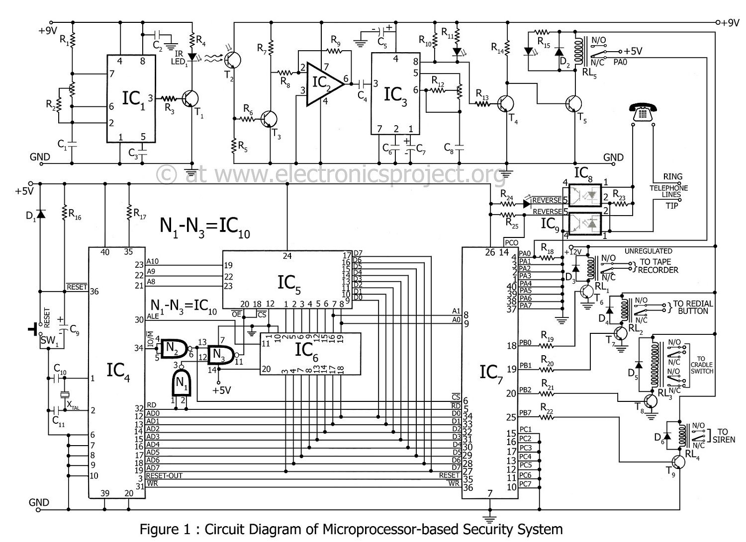
Circuit Diagram Of Microprocessor Based Security System Home Security Home Security Systems Home Security Tips

Pin On Learning Electronics

The 8085 And Its Buses The 8085 Is An 8 Bit General Purpose Microprocessor That Can Address Electronics Basics Programming Tutorial Electrical Circuit Diagram

The Different Types Of Address Decoding Techniques In 8086 Microprocessor Are Absolute Decoding Linear Decoding Block Decoding Decoding Techniques Addressing

Cpu Architecture Computer Architecture Computer Science Architecture

Microprocessors And Microcontrollers Architecture Programming And System Design 8085 8086 8051 8096 Krishna Kant 20 Microcontrollers System Programming

Internal Architecture Of 8085 Microprocessor Electronics Engineering Study Center Electronic Engineering Engineering Data Processing

8085 Microprocessor Working And Its Architecture Central Processing Unit Computer Processor The Unit

Check It Out Output Device Memory Address 8085 Architecture

Pin On The Daily Nerd

At89s52 Microcontroller Pinout Pin Configuration Features Datasheet Microcontrollers Electronic Circuit Projects Circuit Components

Pic 16f887 Based Digital Thermometer Circuit Diagram

Architechture Of 8085 What Is Computer Computer History Computer

Intel 8085 8 Bit Microprocessor 8085 Architecture Intel Diagram Architecture

To Work With Microprocessor 8085 First We Have To Know The Internal Architecture Of 8085 Microproces In 2021 Computer Architecture Electronic Engineering Logic Design

Pin On Knowledge


