The selection of the particular line depends upon the selection line. Heres the module for AND gate with the module name and_gate.

A simple example of an non-electronic circuit of a multiplexer is a single pole multi-position switch.

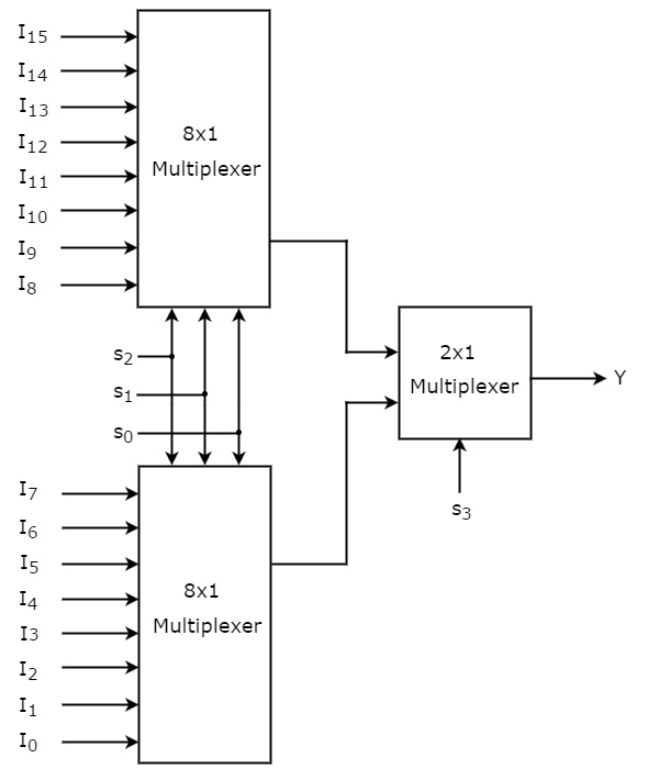
Circuit diagram of 8x1 multiplexer. Mux is a device That has 2n Input Lines. If s 3 is zero then the output of 2x1 Multiplexer will be one of the 8 inputs Is 7 to I 0 based on the values of selection lines s 2 s 1 s 0. From the truth table above we can see that when the data select input A is LOW at logic 0 input I 1 passes its data through the NAND gate multiplexer circuit to the output while input I 0 is blocked.
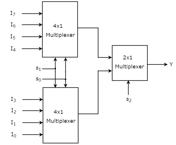
But Only One has Output Line. The data inputs of upper 4x1 Multiplexer are I 7 to I 4 and the data inputs of lower 4x1 Multiplexer are I 3 to I 0. In the circuit when enable pin is set to one the multiplexer will be disabled and if it is zero then select lines will select the corresponding data input to pass through the output.
Multiplexer means many into one. If we have 2 n input lines then n is the selection lines. Where n number of input selector line.
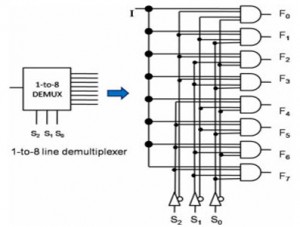
Therefore each 8x1 Multiplexer produces an output based on the values of selection lines s 2 s 1 s 0. The block diagram of 1x8 De-Multiplexer is shown in the following figure. The common selection lines s 1 s 0 are applied to both 1x4 De-Multiplexers.
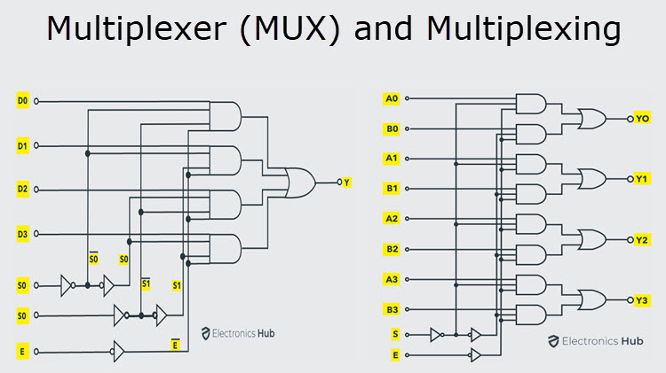
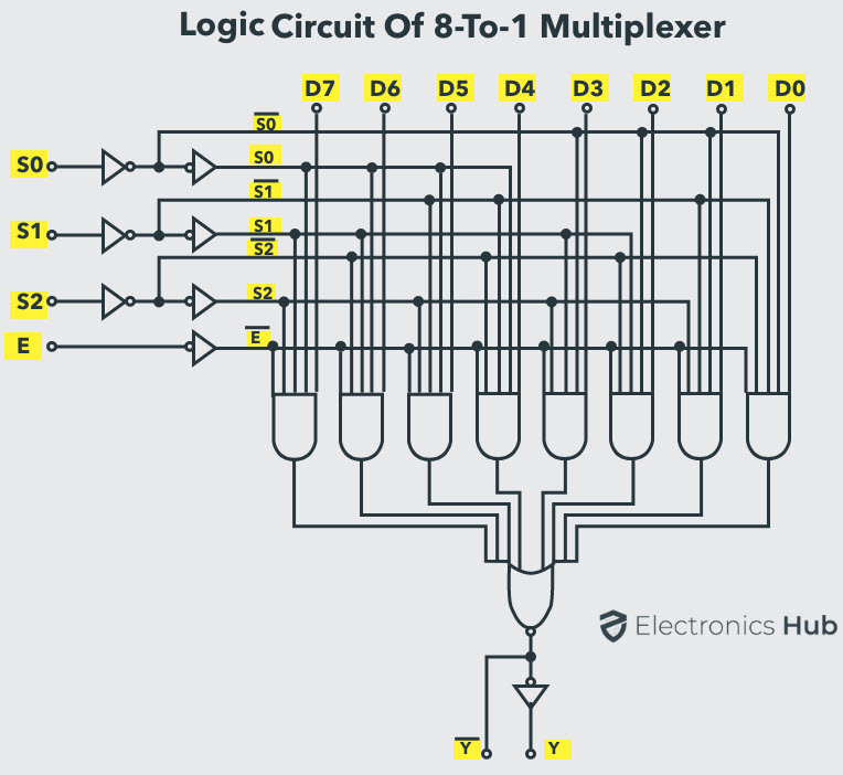
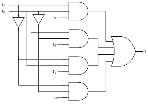
From the above Boolean equation the logic circuit diagram of an 8-to-1 multiplexer can be implemented by using 8 AND gates 1 OR gate and 7 NOT gates as shown in below figure. The block diagram of 8x1 multiplexer is shown in the following figure. Drawing the circuits G A1 A0 B0 A0 B1B0 A1 B1 E A1A0B1B0 A1A0 B1B0 A1 A0 B1 B0 A1 A0B1 B0 L A1A0B0 A0B1 B0 A1B1 LogicWorks has gates with inverted inputs the small bubbles for clearer diagrams.
June 23 2003 Basic circuit design and multiplexers 7 Step 4. The block diagram of 8x1 Multiplexer is shown in the following figure. In This Post I will tell You What is Multiplexer MUX And I am Also will tell you about its working With Logic Diagram And Uses.
B 10 points Assume each 2x1 multiplexer is implemented in SOP form as in Fig. 41c page 190 of the textbook but using CMOS NAND and CMOS NOT gates. A 20 points Draw the circuit diagram of the 8x1 multiplexer.
Firstly I will introduce what is mux. Draw A Circuit Diagram For Multiplexer With 8 Inputstream Posted by Margaret Byrd Posted on December 8 2020 Digital circuits multiplexers multiplexer in electronics design an 8 to 1 line using and demultiplexer types implement logical functions. The port-list will contains the output and input variables.
You can draw a symbol to represent each 2x1 multiplexer and do not need to show its gate-level implementation. A multiplexer is a circuit used to select and route any one of the several input signals to a single output. 16X1 MULTIPLEXER USING 8X1 MULTIPLEXER in simple way In Hindi Electronics Subjectified - YouTube.
The outputs of upper 1x4 De-Multiplexer are Y 7 to Y 4 and the outputs of lower 1x4 De-Multiplexer are Y 3 to Y 0. This abruptly reduces the number of logic gates or integrated circuits to perform the logic function since the multiplexer. The input A of this simple 2-1 line multiplexer circuit constructed from standard NAND gates acts to control which input I 0 or I 1 gets passed to the output at Q.
Multi-position switches are widely used in many electronics circuits. Decide which logical gates you want to implement the circuit with. A multiplexer is a combinational logic circuit that receives 2 n input lines and convert it into a single output line.
However circuits that operate at high speed require the multiplexer to be. Design truth tablelogical expressioncircuit diagram for it duration. The same selection lines s 1 s 0 are applied to both 4x1 Multiplexers.
This is an 8X1 MUX with inputs I0I1I2I3I4I5I6I7 Y as output and S2 S1 S0 as selection lines. No description has been provided for this circuit. In the 81 MUX we need eight AND gates one OR gate and three NOT gates.
Comments 0 Copies 1 8X1 MultiplexerLOGIC DIAGRAM. Logic diagram for 81 MUX Verilog code for 81 mux using structural modeling. What Is Multiplexer And De Multiplexer Types And Its Applications.
The output will depend upon the combination of S2S1 S0 as shown in the. Whos bit combination determines the selected line. Start defining each gate within a module.
The outputs of first stage 8x1 Multiplexers are applied as inputs of 2x1 Multiplexer that is present in second stage. The other selection line s 3 is applied to 2x1 Multiplexer. Since you have mentioned only 4X1 Mux so lets proceed to the answer.
8x1 mux logic diagram.
Multiplexer Mux And Multiplexing
Multiplexer In Digital Electronics Javatpoint
Multiplexer And Demultiplexer Types Differences Their Applications
Plc Program To Implement 8 1 Multiplexer Sanfoundry

Multiplexer In Digital Electronics Electronics Fun
Digital Circuits Multiplexers Tutorialspoint

8 To 1 Function Generator Simple Circuit Computer Memory
Multiplexer And Demultiplexer Types Differences Their Applications
Multiplexer Mux And Multiplexing

Circuitverse 8x1 Multiplexer

8 Input Multiplexer Youtube
Multiplexer Mux And Multiplexing
Digital Circuits Multiplexers Tutorialspoint

Vhdl Code For 8 To 1 Multiplexer And 1 To 8 Demultiplexer Engineering Notes
Digital Circuits Multiplexers Tutorialspoint

Multiplexer Mux And Multiplexing Digital Technology Circuit Digital

Multiplexer What Is It And How Does It Work Electrical4u

Multiplexer Truth Table 8 To 1
8 Input Multiplexer Multisim Live


